- 您现在的位置:买卖IC网 > Sheet目录985 > ISLA224IR72EV1Z (Intersil)BOARD EVALUATION FOR ISLA224P
�� �
�
�ISLA224P�
�TABLE� 7.� MEDIUM� AND� FINE� GAIN� ADJUSTMENTS�
�Global� Device� Configuration/Control�
�PARAMETER�
�Steps�
�–Full� Scale� (0x00)�
�Mid–Scale� (0x80)�
�+Full� Scale� (0xFF)�
�Nominal� Step� Size�
�0x23[7:0]�
�MEDIUM� GAIN�
�256�
�-2%�
�0.00%�
�+2%�
�0.016%�
�0x24[7:0]�
�FINE� GAIN�
�256�
�-0.20%�
�0.00%�
�+0.2%�
�0.0016%�
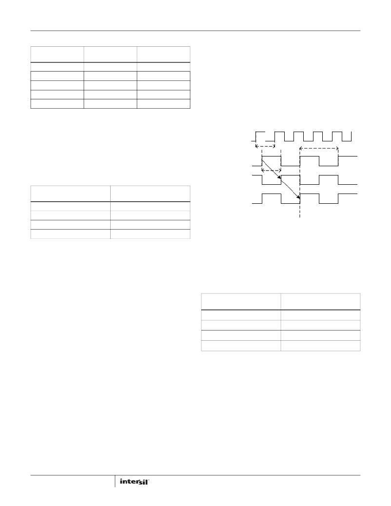
�ADDRESS� 0X71:� PHASE_SLIP�
�The� output� data� clock� is� generated� by� dividing� down� the� A/D� input�
�sample� clock.� Some� systems� with� multiple� A/Ds� can� more� easily� latch�
�the� data� from� each� A/D� by� controlling� the� phase� of� the� output� data�
�clock.� This� control� is� accomplished� through� the� use� of� the� phase_slip�
�SPI� feature,� which� allows� the� rising� edge� of� the� output� data� clock� to� be�
�advanced� by� one� input� clock� period,� as� shown� in� the� Figure� 44.�
�Execution� of� a� phase_slip� command� is� accomplished� by� first� writing� a�
�ADDRESS� 0X25:� MODES�
�Two� distinct� reduced� power� modes� can� be� selected.� By� default,�
�the� tri-level� NAPSLP� pin� can� select� normal� operation,� nap� or�
�sleep� modes� (refer� to“Nap/Sleep”� on� page� 20).� This� functionality�
�'0'� to� bit� 0� at� address� 0x71,� followed� by� writing� a� '1'� to� bit� 0� at� address�
�0x71.�
�ADC� Input�
�Clock� (500MHz)�
�can� be� overridden� and� controlled� through� the� SPI.� This� is� an�
�indexed� function� when� controlled� from� the� SPI,� but� a� global�
�function� when� driven� from� the� pin.� This� register� is� not� changed� by�
�a� Soft� Reset.�
�TABLE� 8.� POWER-DOWN� CONTROL�
�0x25[2:0]�
�VALUE�
�POWER� DOWN� MODE�
�000�
�Pin� Control�
�001�
�Normal� Operation�
�Output� Data�
�Clock� (250MHz)�
�No� clock_slip�
�Output� Data�
�Clock� (250MHz)�
�1� clock_slip�
�Output� Data�
�Clock� (250MHz)�
�2� clock_slip�
�2ns�
�2ns�
�4ns�
�010�
�100�
�Nap� Mode�
�Sleep� Mode�
�FIGURE� 44.� PHASE� SLIP�
�ADDRESS� 0X72:� CLOCK_DIVIDE�
�ADDRESS� 0X26:� OFFSET_COARSE_ADC1�
�ADDRESS� 0X27:� OFFSET_FINE_ADC1�
�The� input� offset� of� A/D� core#1� can� be� adjusted� in� fine� and�
�coarse� steps� in� the� same� way� that� offset� for� core#0� can� be�
�adjusted.� Both� adjustments� are� made� via� an� 8-bit� word� as�
�detailed� in� Table� 5.� The� data� format� is� two’s� complement.�
�The� ISLA224P25� has� a� selectable� clock� divider� that� can� be� set� to�
�divide� by� two� or� one� (no� division).� By� default,� the� tri-level� CLKDIV�
�pin� selects� the� divisor� This� functionality� can� be� overridden� and�
�controlled� through� the� SPI,� as� shown� in� Table� 9.� This� register� is�
�not� changed� by� a� Soft� Reset.�
�TABLE� 9.� CLOCK� DIVIDER� SELECTION�
�The� default� value� of� each� register� will� be� the� result� of� the�
�self-calibration� after� initial� power-up.� If� a� register� is� to� be�
�incremented� or� decremented,� the� user� should� first� read� the�
�register� value� then� write� the� incremented� or� decremented� value�
�back� to� the� same� register.� Bit� 0� in� register� 0xFE� must� be� set� high�
�to� enable� updates� written� to� 0x26� and� 0x27� to� be� used� by� the�
�ADC� (see� description� for� 0xFE).�
�VALUE�
�000�
�001�
�010�
�other�
�0x72[2:0]�
�CLOCK� DIVIDER�
�Pin� Control�
�Divide� by� 1�
�Divide� by� 2�
�Not� Allowed�
�ADDRESS� 0X28:� GAIN_COARSE_ADC1�
�ADDRESS� 0X29:� GAIN_MEDIUM_ADC1�
�ADDRESS� 0X2A:� GAIN_FINE_ADC1�
�Gain� of� A/D� core� #1� can� be� adjusted� in� coarse,� medium� and� fine�
�steps� in� the� same� way� that� core� #0� can� be� adjusted.� Coarse� gain� is�
�a� 4-bit� adjustment� while� medium� and� fine� are� 8-bit.� Multiple�
�Coarse� Gain� Bits� can� be� set� for� a� total� adjustment� range� of� ±4.2.�
�Bit� 0� in� register� 0xFE� must� be� set� high� to� enable� updates� written� to�
�0x29� and� 0x2A� to� be� used� by� the� ADC� (see� description� for� 0xFE).�
�26�
�ADDRESS� 0X73:� OUTPUT_MODE_A�
�The� output_mode_A� register� controls� the� physical� output� format�
�of� the� data,� as� well� as� the� logical� coding.� The� ISLA224P25� can�
�present� output� data� in� two� physical� formats:� LVDS(default)� or�
�LVCMOS.� Additionally,� the� drive� strength� in� LVDS� mode� can� be� set�
�high� (default,� 3mA� or� low� (2mA).�
�Data� can� be� coded� in� three� possible� formats:� two’s�
�complement(default),� Gray� code� or� offset� binary.� See� Table� 11.�
�This� register� is� not� changed� by� a� Soft� Reset.�
�FN7570.1�
�November� 30,� 2012�
�发布紧急采购,3分钟左右您将得到回复。
相关PDF资料
ISPTPKIT
SCREW KIT TAMPER RESISTANT 9PCS
ITCSN-0400-25-U
HEATSHRINK ITCSN 2/5" X 25'
JC2AF-TM-DC24V-F
RELAY GEN PURPOSE DPST 10A 24V
JJM1A-12V
RELAY AUTOMOTIVE SPST 20A 12V
JM1AN-ZTM-DC5V-F
RELAY GEN PURPOSE SPST 20A 5V
JQ1P-18V-F
RELAY GEN PURPOSE SPDT 10A 18V
JS1-F-6V-F
RELAY GEN PURPOSE SPDT 10A 6V
JSM1-9V-5
RELAY AUTOMOTIVE SPDT 15A 9V
相关代理商/技术参数
ISLA224P
制造商:INTERSIL 制造商全称:Intersil Corporation 功能描述:Dual 14-Bit, 250MSPS/200MSPS/130MSPS ADC
ISLA224P12
制造商:INTERSIL 制造商全称:Intersil Corporation 功能描述:High Performance Dual 14-Bit, 125MSPS ADC
ISLA224P12IRZ
制造商:Intersil Corporation 功能描述:DUAL 14-BIT 125MSPS UNBUFFERED INPUT, 72-PIN - Trays 制造商:Intersil Corporation 功能描述:IC ADC 14BIT SPI/SRL 125M 48QFN 制造商:Intersil 功能描述:Dual 14-Bit 125MSPS Unbuffered Input, 72
ISLA224P13
制造商:INTERSIL 制造商全称:Intersil Corporation 功能描述:Dual 14-Bit, 250MSPS/200MSPS/130MSPS ADC
ISLA224P13IRZ
制造商:Intersil Corporation 功能描述:DUAL 14-BIT 130MSPS UNBUFFERED INPUT, 72-PIN - Trays 制造商:Intersil Corporation 功能描述:IC ADC 14BIT SRL/SPI 72QFN 制造商:Intersil 功能描述:DL 14-BIT 130MSPS UNBUFRED INPUT 72PIN
ISLA224P20
制造商:INTERSIL 制造商全称:Intersil Corporation 功能描述:Dual 14-Bit, 250MSPS/200MSPS/130MSPS ADC
ISLA224P20IRZ
制造商:Intersil Corporation 功能描述:DUAL 14-BIT 200MSPS UNBUFFERED INPUT, 72-PIN - Trays 制造商:Intersil Corporation 功能描述:IC ADC 14BIT SRL/SPI 72QFN 制造商:Intersil 功能描述:DL 14-BIT 200MSPS UNBUFRED INPUT 72PIN 制造商:Intersil Corporation 功能描述:IC, ADC, 14BIT; Resolution (Bits):14bit; Sampling Rate:200MSPS; Supply Voltage Type:Single; Supply Voltage Min:1.7V; Supply Voltage Max:1.9V; Supply Current:375mA; Digital IC Case Style:QFN; No. of Pins:72; Data Interface:SPI ;RoHS Compliant: Yes
ISLA224P25
制造商:INTERSIL 制造商全称:Intersil Corporation 功能描述:Dual 14-Bit, 250MSPS/200MSPS/130MSPS ADC